ADC (Analog to Digital Converter) in AVR
Blog #DSS003 Introduction to ADC An ADC is used to convert an analogue signal such as a DC voltage to
Blog #DSS003 Introduction to ADC An ADC is used to convert an analogue signal such as a DC voltage to

Blog #DSS003
An ADC is used to convert an analogue signal such as a DC voltage to a digital form.
The same digital form (binary format) will be processed to micro controller.
What is Analog to Digital converter?
Analog to Digital conversion (ADC) is an electronic process in which a continuously a voltage (Analog
Signal) is changed into multilevel digital signal without altering its essential content.
This converter changes a signal in terms of time and amplitude to a digital signal in terms of both time and amplitude.
The output of the analog-to-digital converter has defined levels or states. The number of states is almost always a power of two.
The ADC analog signal into digital signal at some regular interval which is determined by the clock frequency. In general, the ADC operates within a frequency range of 50kHz to 200kHz. But the CPU clock frequency is much higher (measure to MHz). Which can be achieved with frequency division. The prescaler acts as frequency division factor. It produces desired frequency from the external higher frequency. There are some predefined division factors – 2, 4, 8, 16, 32, 64, and 128. For example, a prescaler of 64 implies F_ADC = F_CPU/64. For F_CPU = 16MHz, F_ADC = 16M/64 = 250kHz.
“Greater the frequency, lesser the accuracy and vice-versa”
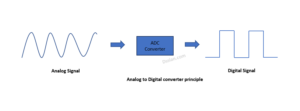
Digital signals propagate more efficiently than analog signal, largely because digital impulses are well-defined and orderly.
The AVR (ATMEGA32/ATMEGA16) PORTA contains ADC pins. The ADC features in AVR as below,
As you can from the above point 1, AVR has 8 channels 10-bit resolution.
8 channels states there are 8 ADC pins are multiplexed together in PORT A of ATMEGA16/32.
10-bit resolution states there are 2^10 = 1,024 steps,
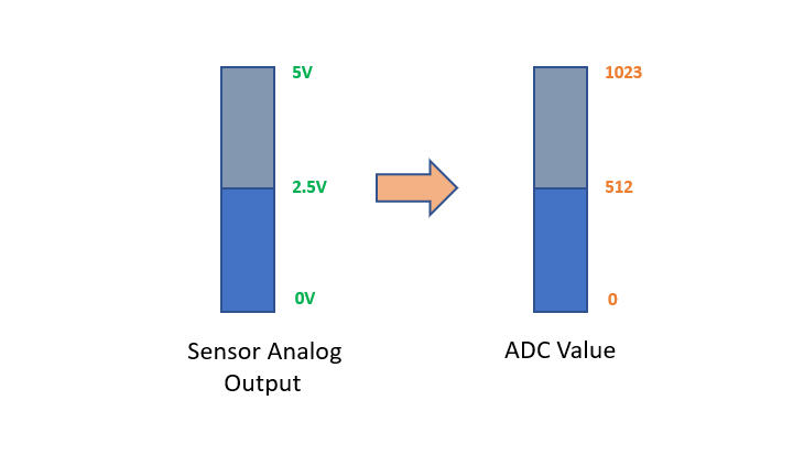
ADC reads 5V called analog value. Any analog value in between 0V and 5V is converted into its
equivalent ADC value.
The 0V to 5V range is divided into 2^10 = 1,024 steps. Thus ,

These bits select the voltage reference for the ADC.If these bits are
changed during a conversion, the change will not go in effect until this conversion is complete.

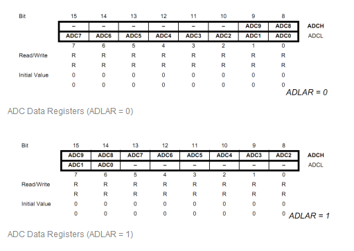
Make it ‘1’ to Left Adjust the ADC Result.Changing the ADLAR bit will affect the ADC Data Register immediately.
ADLAR – 1 to left adjust the result and ADLAR – 0 to rtight adjust the result.
This bit is to select ADC channel.Its is of 5 bits, hence 2^5 = 32 different conditions as below. By default all the bits are 0.
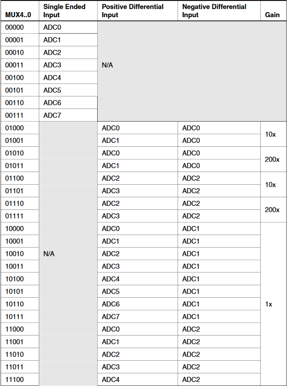

ADMUX initialization : ADMUX = (1<<REFS0);

It enables the ADC feature. If it is not enabled then the PORTA will be have as GPIO.The ADC is enabled by setting the ADC Enable bit, ADEN in ADCSRA. Voltage reference and input channel selections will not go into effect until ADEN is set. The ADC does not consume power when ADEN is cleared, so it is recommended to switch off the ADC before entering power saving sleep modes.
Write this to ‘1’ before starting any conversion.if ADSC is written at the same time as the ADC is enabled,will take 25 ADC clock cycles instead of the normal 13.This first conversion performs initialization of the ADC.ADSC will read as one as long as a conversion is in progress. When the conversion is complete,it returns to zero. Writing zero to this bit has no effect.
When this bit is written to one, Auto Triggering of the ADC is enabled.The trigger source is selected by settingthe ADC Trigger Select bits, ADTS in SFIOR.
This bit is set when an ADC conversion completes and the Data Registers are updated.The ADC Conversion Complete Interrupt is executed if the ADIE bit and the I-bit in SREG are set.
ADIF is cleared by hardware when executing the corresponding interrupt handling vector.ADIF is cleared by writing a logical one to the flag.
When this bit is written to one and the I-bit in SREG is set.The ADC Conversion Complete Interrupt is activated.
These bits determine the division factor between the XTAL frequency and the input clock to the ADC.
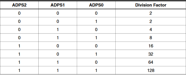
For AVR(ATMEGA16/32) the crystal frequency 16MHz and the frequency range of 50kHz-200kHz so the prescaler is 128.
F_ADC = 16M/128 = 125kHz. Now we will initialize ADCSRA.
ADCSRA = (1<<ADEN)|(1<<ADPS2)|(1<<ADPS1)|(1<<ADPS0);
// prescaler = 128
The ADC generates a 10-bit result which is presented in the ADC Data Registers, ADCH and ADCL. By default, the result is presented right adjusted, but can optionally be presented left adjusted by setting the ADLAR bit in ADMUX.If the result is left adjusted and no more than 8-bit precision is required, it is sufficient to read ADCH. Otherwise, ADCL must be read first, then ADCH, to ensure that the content of the Data
Registers belongs to the same conversion. Once ADCL is read, ADC access to Data Registers is blocked. This means that if ADCL has been read, and a conversion completes before ADCH is read, neither register is updated and the result from the conversion is lost. When ADCH is read,ADC access to the ADCH and ADCL Registers is re-enabled.
After the conversion is complete (ADIF is high), the conversion result can be found in the ADC Result Registers (ADCL, ADCH). For single ended conversion, the result is, 
When differential channels are used, the result is, ![]()
The ADC conversion result shall store in ADCL and ADCH. AVR has 10-bit ADC resolution, it required 10 bits to store result. As single 8 bit is not sufficient it is required to 2 registers ADCL (LOW Byte) and ADCH (HIGH Byte). ADLAR = 1 left selected, ADLAR = 0 right selected.
The register is enabled when ADATE (in ADCSRA) is set to ‘1’. Usually this bit is ‘0’.

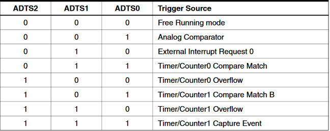
When ADATE in ADCSRA is set then the source shall be selected as per ADTS settings for ADC conversion. If ADATE is reset then no effect to ADTS settings.
void adc_init()
{
ADMUX = (1<<REFS0);// AREF = AVcc
ADCSRA = (1<<ADEN)|(1<<ADPS2)|(1<<ADPS1)|(1<<ADPS0); /* ADC Enable and prescaler of 128 “16000000/128 = 125000” */
}
uint16_t adcSignalRead(uint8_t channel)
{
channel &= 0b00000111; /* Select the ADC channel by AND operation with 7 */
ADMUX = (ADMUX & 0xF8) | channel; /* clears the bottom 3 bits before */
ADCSRA |= (1<<ADSC); /* start single convertion */
while(ADCSRA & (1<<ADSC));
return (ADC);
}
Now you can refer to the link for example sensor interfacing with AVR,
Interfacing water sensor with AVR – DSS (dssian.com)
Also, you can refer to the dataset available in link – ATmega32A Datasheet (microchip.com) for more details.
Very nice and detail explanation on ADC
Can you write an article for a input capture mode and how to find the frequency and the pwm duty cycle
Dear Ravikant,
Thank you very much. We have noted your request and will make sure to notify you when the topic is published.
Definitely believe that which you stated.
Your favorite reeason seemed to be at the web the easest thing to keep in mind of.
I say to you, I certainly get annoyed whilst people consider issues that they just do nott recognise about.
You managed to hit the nail upon the highest as neatly as outlined
out the whole thing with no need side-effects ,
other people could take a signal. Will probably be again to geet more.
Thank you
Here is my blog https://casinovavada.blogspot.com/2021/12/blog-post_22.html
I’ve been browsing on-line more than 3 hours as of late, but I never found any fascinating article like yours.
It’s pretty price enough for me. In my view, if all web
owners and bloggers made excellent content material as
you probably did, the web shall be a lot more helpful thhan ever
before.
My blpg post – Forum.Ll2.Ru
I can’t help but feel that this is the kind of work that will stand the test of time. There’s a timeless quality to your writing that transcends trends and fads. It’s the kind of piece that people will look back on years from now and still find meaning in.
Blog DSS#002 On these days water level indicator provides a great relieve with its simple mechanism. It is as simple
Blog DSS#002
On these days water level indicator provides a great relieve with its simple mechanism. It is as simple as detect and indicate water level in water tank / water reservoir by activating applied features. Some can detect water load and enable/disable pump eclectic supply, or some can blow alarm beyond water level.
” Water level sensor working principle is when the sensor is sensing water or put into certain depth, the pressure on the sensor’s lower layer converted into water level height. The calculated formula is Ρ=ρ.g.H+Po, ” Where P is Pressure on the sensor’s lower layer, ρ is the density of water, Po is the atmospheric pressure of water surface area, g is acceleration to the gravity, H is the depth at which the sensor inside water level.
There are different types of water level sensor which is used based on application to application. Other types of water level sensors can be found in https://google.com or we will update in future if we have demonstrated any other water level sensor.
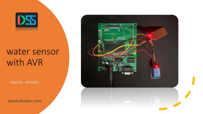
Water level sensor has 3 pins (VCC 5v [+], GND [-], Source [Analog Input]). You can see below picture for connections. This code is implemented as when water sensor detects water level (Touch to liquid) it activates PORTD PIN0. This PIN0 is connected to relay module (5V). You can feel a delay in response while reading signal and enable/disable relay due delay mechanism. It is required to give some delay of sensing the water to ensure constant water and delay time also helps relay to power ON pump or power OFF pump.

/*
 * ADCinAVR.c
 *
 * Created: 5/18/2023 9:44:14 PM
 * Author : DSSIAN
   License : STUDENT
   Copyrights : DSSIAN
 */

#define F_CPU 16000000UL
#include <avr/io.h>
#include <util/delay.h>

#define ANALOG_READTHRESHLD 150u
#define SIGNAL_OFF 0x00
#define SIGNAL_ON 0x01
#define Pump_swt PORTD

uint16_t WaterSensor1_ReadData = 0u;
uint16_t WaterSensor2_ReadData = 0u; /* Defined for future implementation */

void adc_init()
{
	// AREF = AVcc
	ADMUX = (1<<REFS0);

	// ADC Enable and prescaler of 128
	// 16000000/128 = 125000
	ADCSRA = (1<<ADEN)|(1<<ADPS2)|(1<<ADPS1)|(1<<ADPS0);
}

uint16_t adc_read(uint8_t ch)
{
	// select the corresponding channel 0~7
	// ANDing with '7' will always keep the value
	// of 'ch' between 0 and 7
	ch &= 0b00000111;  // AND operation with 7
	ADMUX = (ADMUX & 0xF8)|ch;     // clears the bottom 3 bits before ORing

	// start single conversion
	// write '1' to ADSC
	ADCSRA |= (1<<ADSC);

	// wait for conversion to complete
	// ADSC becomes '0' again
	// till then, run loop continuously
	while(ADCSRA & (1<<ADSC));

	return (ADC);
}

void PumpControl_SignalReceiveData(uint16_t WaterSensor_ReadData)
{
    WaterSensor1_ReadData = WaterSensor_ReadData;

	if(WaterSensor_ReadData>ANALOG_READTHRESHLD)
	Pump_swt = SIGNAL_OFF;
	else
	{
		_delay_ms(500);
		Pump_swt = SIGNAL_ON;
	}
	//Pump_swt = SIGNAL_ON;


}
int main(void)
{
	uint16_t adc_result0;

	 DDRD = 0x01;           // to connect led to PC0
	  adc_init();
	  _delay_ms(50);

    /* Replace with your application code */
    while(1)
    {
		adc_result0 = adc_read(0);      // read adc value at PA0
		PumpControl_SignalReceiveData(adc_result0);
	}
}
All these components are available at https://robu.in/. The price and quality of component quite good here with my experience but you can buy where you are comfortable.
2024 is the revolution for IOT (Internet of things). The market is getting spread to explore IOT technology for their
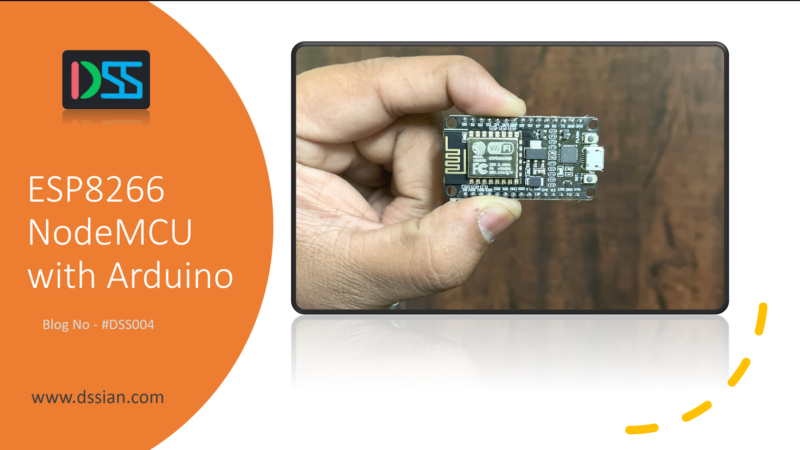
2024 is the revolution for IOT (Internet of things). The market is getting spread to explore IOT technology for their respective businesses. Every business is looking for the opportunity to implement IOT technology and some are already leading the market. As the market is already leading this technology and some are exploring to make it better to excellence, the semiconductor companies are coming up with multiple ICs and the development boards. In this NodeMCU is one of best IOT development board to explore IOT solutions. NodeMCU is a board name or a variant with ESP8266 Wi-Fi microcontroller. Something is going on your mind now, right? Yes, ESP8266 is also a microcontroller. This electronic component ESP8266 is a microcontroller solution which has at least minimum jobs like GPIO, ADC,serial communication, flash memory, RAM as per other microcontrollers.
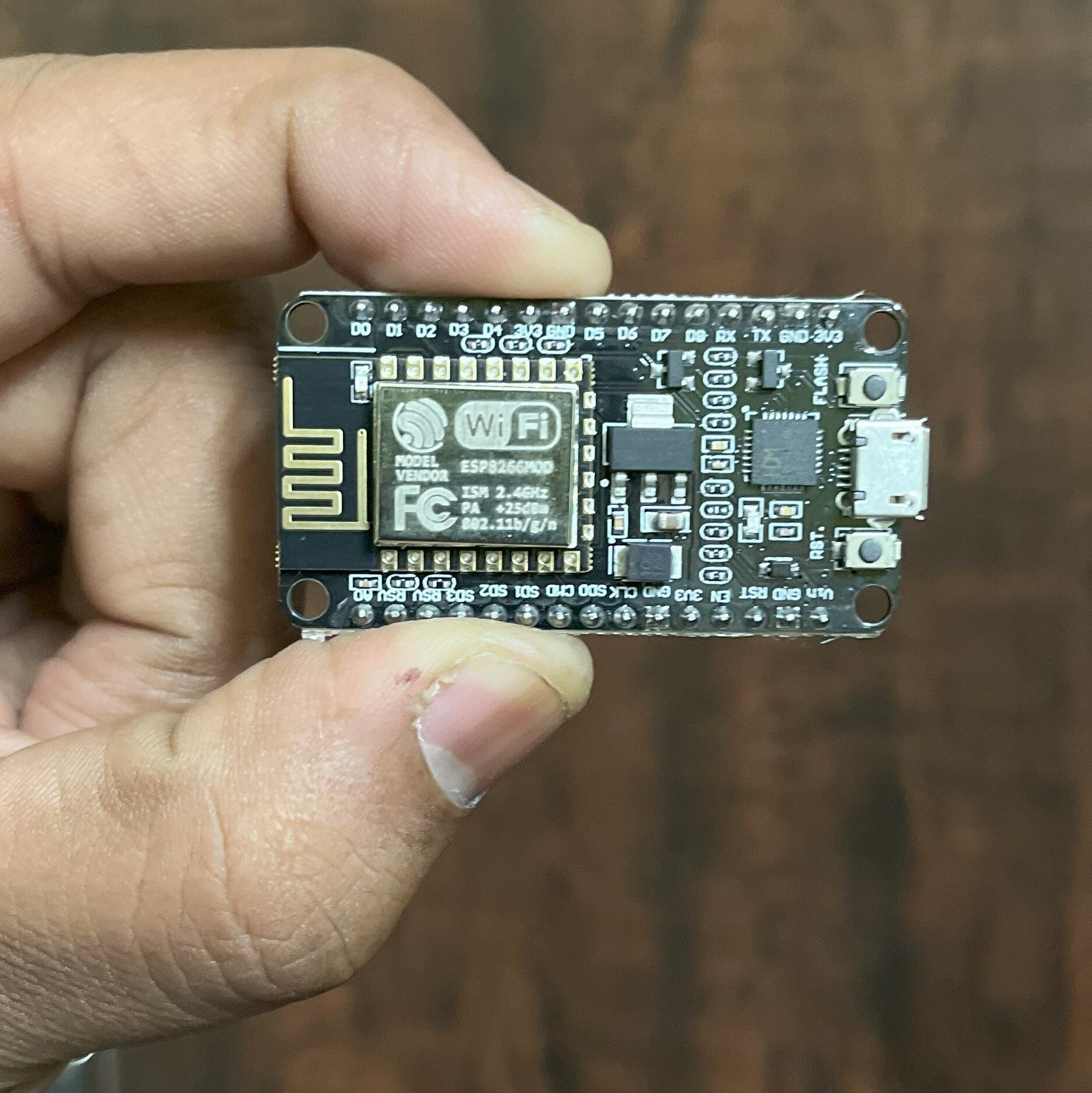
NodeMCU is an open source IOT platform based on Espressif ESP8266 SoC system. It is also an open-source firmware to design different IOT based prototypes or the solutions. This standalone device can be also used as Wi-Fi router to create a wireless network. Other devices or microcontrollers are connected as client to NodeMCU (SSID, Password).
There are two available versions of NodeMCU as version 0.9 & 1.0 where the version 0.9 contains ESP-12 and version 1.0 contains ESP-12E where E stands for “Enhanced”. Espressif also has ESP8266 SoC based another device called ESP32.
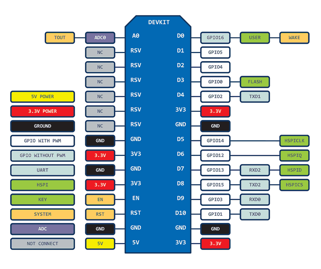
Once after successful installation of Arduino IDE (Follow references link to install Arduino IDE, Drivers, etc.), configure the IDE as below,
Step 1: Arduino IDE -> File – > Preferences – paste the below URL,
“http://arduino.esp8266.com/stable/package_esp8266com_index.json”


Step 2 : Tools -> Board -> Board Manager
Search ESP8266 device and install with right version. This will add ESP8266 board to arduino IDE.
Step 3: Now to recognize the nodemcu board on computer install the CP210x driver. Link can be found in below references tab.

Step 4: Select the ESP8266 board.
Tools -> Board -> esp8266 -> NodeMCU 1.0(ESP-12E Module)

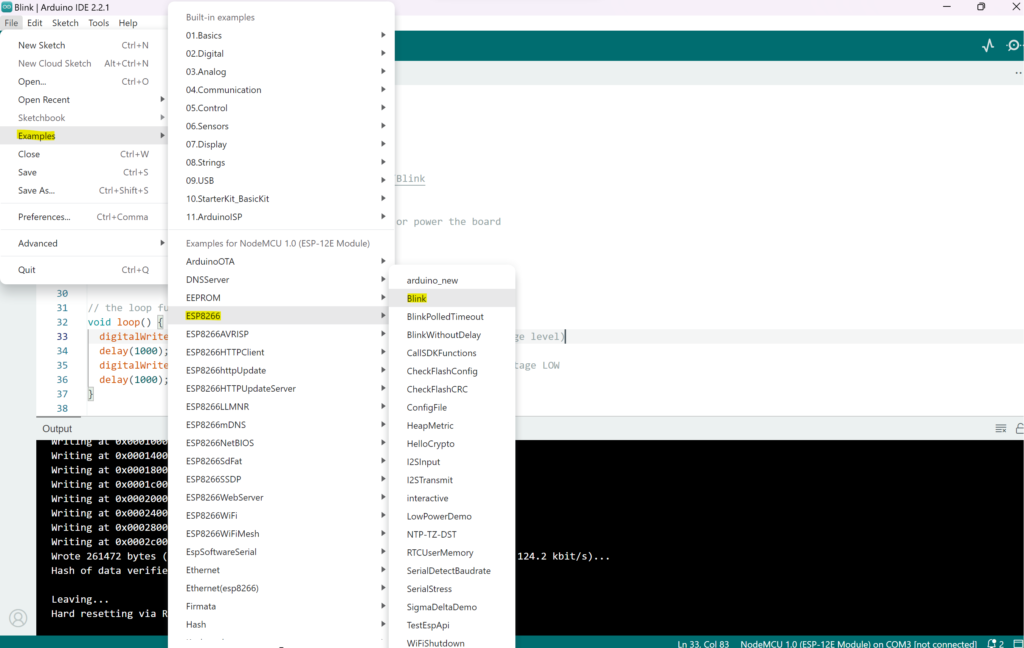
Step 5: Test the nodemcu by blinking the led.
File – > Example -> ESP8266 -> Blink
Step 6: Now compile the code and flash to NodeMCU.
RRw jYUvpy sAThg WhvNn WptrMJD Qayde
Leave a Reply