

Blog #DSS003
Introduction to ADC
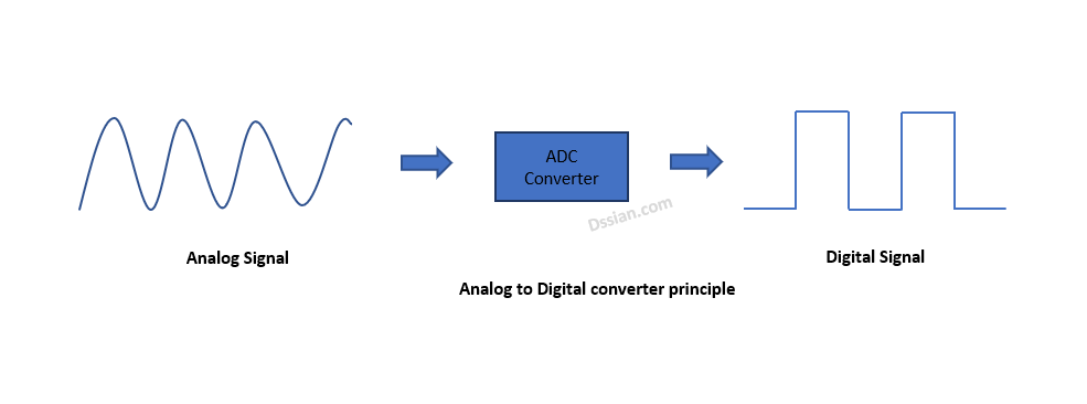
An ADC is used to convert an analogue signal such as a DC voltage to a digital form.
The same digital form (binary format) will be processed to micro controller.
What is Analog to Digital converter?
Analog to Digital conversion (ADC) is an electronic process in which a continuously a voltage (Analog
Signal) is changed into multilevel digital signal without altering its essential content.
This converter changes a signal in terms of time and amplitude to a digital signal in terms of both time and amplitude.
The output of the analog-to-digital converter has defined levels or states. The number of states is almost always a power of two.
ADC Prescaler
The ADC analog signal into digital signal at some regular interval which is determined by the clock frequency. In general, the ADC operates within a frequency range of 50kHz to 200kHz. But the CPU clock frequency is much higher (measure to MHz). Which can be achieved with frequency division. The prescaler acts as frequency division factor. It produces desired frequency from the external higher frequency. There are some predefined division factors – 2, 4, 8, 16, 32, 64, and 128. For example, a prescaler of 64 implies F_ADC = F_CPU/64. For F_CPU = 16MHz, F_ADC = 16M/64 = 250kHz.
“Greater the frequency, lesser the accuracy and vice-versa”
Digital signals propagate more efficiently than analog signal, largely because digital impulses are well-defined and orderly.
ADC in AVR
The AVR (ATMEGA32/ATMEGA16) PORTA contains ADC pins. The ADC features in AVR as below,
As you can from the above point 1, AVR has 8 channels 10-bit resolution.
8 channels states there are 8 ADC pins are multiplexed together in PORT A of ATMEGA16/32.
10-bit resolution states there are 2^10 = 1,024 steps,
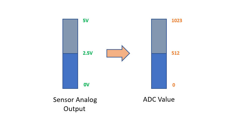
ADC reads 5V called analog value. Any analog value in between 0V and 5V is converted into its
equivalent ADC value.
The 0V to 5V range is divided into 2^10 = 1,024 steps. Thus ,
- 0V input will be 0 ADC output
- 2.5V input will be 512 ADC output
- 5V input will be 1023 ADC output
Hence it’s called Successive Approximation ADC type in AVR MCU.
The ADC contains a Sample and Hold circuit which ensures that the input voltage to the ADC is
held at a constant level during conversion. The ADC has a separate analog supply voltage pin, AVCC. AVCC must not differ more than
±0.3V from VCC .
Now we need to understand ” HOW AVR MCU considers the signal is a ADC Signal ?”
Before that you need to also understand ADC Prescaler (explained at beginning) and ADC Registers.
ADC Registers
ADMUX – ADC Multiplexer Selection Register
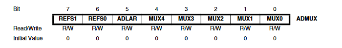
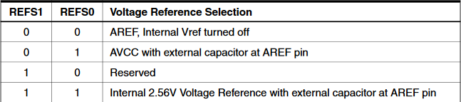
Bits 7:6 – REFS1:0 – Reference Selection Bits
These bits select the voltage reference for the ADC.If these bits are
changed during a conversion, the change will not go in effect until this conversion is complete.
Bit 5 – ADLAR: ADC Left Adjust Result
Make it ‘1’ to Left Adjust the ADC Result.Changing the ADLAR bit will affect the ADC Data Register immediately.
ADLAR – 1 to left adjust the result and ADLAR – 0 to rtight adjust the result.
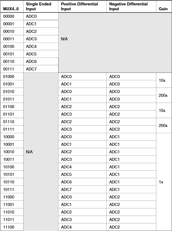
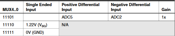
Bits 4:0 – MUX4:0: Analog Channel and Gain Selection Bits
This bit is to select ADC channel.Its is of 5 bits, hence 2^5 = 32 different conditions as below. By default all the bits are 0.
ADMUX initialization : ADMUX = (1<<REFS0);
ADCSRA – ADC Control and Status Register A
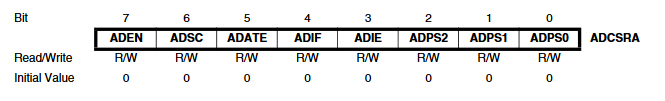
Bit 7 – ADEN – ADC Enable
It enables the ADC feature. If it is not enabled then the PORTA will be have as GPIO.The ADC is enabled by setting the ADC Enable bit, ADEN in ADCSRA. Voltage reference and input channel selections will not go into effect until ADEN is set. The ADC does not consume power when ADEN is cleared, so it is recommended to switch off the ADC before entering power saving sleep modes.
Bit 6 – ADSC: ADC Start Conversion
Write this to ‘1’ before starting any conversion.if ADSC is written at the same time as the ADC is enabled,will take 25 ADC clock cycles instead of the normal 13.This first conversion performs initialization of the ADC.ADSC will read as one as long as a conversion is in progress. When the conversion is complete,it returns to zero. Writing zero to this bit has no effect.
Bit 5 – ADATE: ADC Auto Trigger Enable
When this bit is written to one, Auto Triggering of the ADC is enabled.The trigger source is selected by settingthe ADC Trigger Select bits, ADTS in SFIOR.
Bit 4 – ADIF: ADC Interrupt Flag
This bit is set when an ADC conversion completes and the Data Registers are updated.The ADC Conversion Complete Interrupt is executed if the ADIE bit and the I-bit in SREG are set.
ADIF is cleared by hardware when executing the corresponding interrupt handling vector.ADIF is cleared by writing a logical one to the flag.
Bit 3 – ADIE: ADC Interrupt Enable
When this bit is written to one and the I-bit in SREG is set.The ADC Conversion Complete Interrupt is activated.
Bits 2:0 – ADPS2:0: ADC Prescaler Select Bits
These bits determine the division factor between the XTAL frequency and the input clock to the ADC.
ADC Prescaler Selections
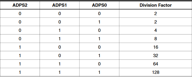
For AVR(ATMEGA16/32) the crystal frequency 16MHz and the frequency range of 50kHz-200kHz so the prescaler is 128.
F_ADC = 16M/128 = 125kHz. Now we will initialize ADCSRA.
ADCSRA = (1<<ADEN)|(1<<ADPS2)|(1<<ADPS1)|(1<<ADPS0);
// prescaler = 128
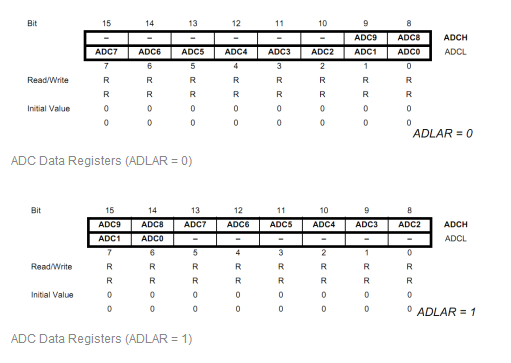
ADCL and ADCH – ADC Data Registers
The ADC generates a 10-bit result which is presented in the ADC Data Registers, ADCH and ADCL. By default, the result is presented right adjusted, but can optionally be presented left adjusted by setting the ADLAR bit in ADMUX.If the result is left adjusted and no more than 8-bit precision is required, it is sufficient to read ADCH. Otherwise, ADCL must be read first, then ADCH, to ensure that the content of the Data
Registers belongs to the same conversion. Once ADCL is read, ADC access to Data Registers is blocked. This means that if ADCL has been read, and a conversion completes before ADCH is read, neither register is updated and the result from the conversion is lost. When ADCH is read,ADC access to the ADCH and ADCL Registers is re-enabled.
After the conversion is complete (ADIF is high), the conversion result can be found in the ADC Result Registers (ADCL, ADCH). For single ended conversion, the result is, 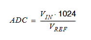
When differential channels are used, the result is, 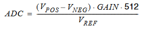
The ADC conversion result shall store in ADCL and ADCH. AVR has 10-bit ADC resolution, it required 10 bits to store result. As single 8 bit is not sufficient it is required to 2 registers ADCL (LOW Byte) and ADCH (HIGH Byte). ADLAR = 1 left selected, ADLAR = 0 right selected.
SFIOR – Special Function I/O Register
The register is enabled when ADATE (in ADCSRA) is set to ‘1’. Usually this bit is ‘0’.
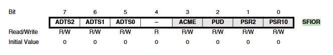
ADC Auto Trigger Source – ADTS
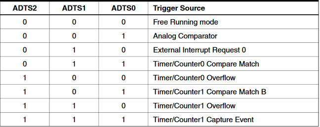
When ADATE in ADCSRA is set then the source shall be selected as per ADTS settings for ADC conversion. If ADATE is reset then no effect to ADTS settings.
ADC programming
ADC Initialization:
void adc_init()
{
ADMUX = (1<<REFS0);// AREF = AVcc
ADCSRA = (1<<ADEN)|(1<<ADPS2)|(1<<ADPS1)|(1<<ADPS0); /* ADC Enable and prescaler of 128 “16000000/128 = 125000” */
}
ADC Read data Function:
uint16_t adcSignalRead(uint8_t channel)
{
channel &= 0b00000111; /* Select the ADC channel by AND operation with 7 */
ADMUX = (ADMUX & 0xF8) | channel; /* clears the bottom 3 bits before */
ADCSRA |= (1<<ADSC); /* start single convertion */
while(ADCSRA & (1<<ADSC));
return (ADC);
}
Now you can refer to the link for example sensor interfacing with AVR,
Interfacing water sensor with AVR – DSS (dssian.com)
Also, you can refer to the dataset available in link – ATmega32A Datasheet (microchip.com) for more details.
Responses
-
Very nice and detail explanation on ADC
Can you write an article for a input capture mode and how to find the frequency and the pwm duty cycle -
Dear Ravikant,
Thank you very much. We have noted your request and will make sure to notify you when the topic is published.
-
kfy4y1
Leave a Reply